- 您现在的位置:买卖IC网 > Sheet目录369 > W971GG6JB25I (Winbond Electronics)IC DDR2 SDRAM 1GBIT 84WBGA
�� �
�
�W971GG6JB�
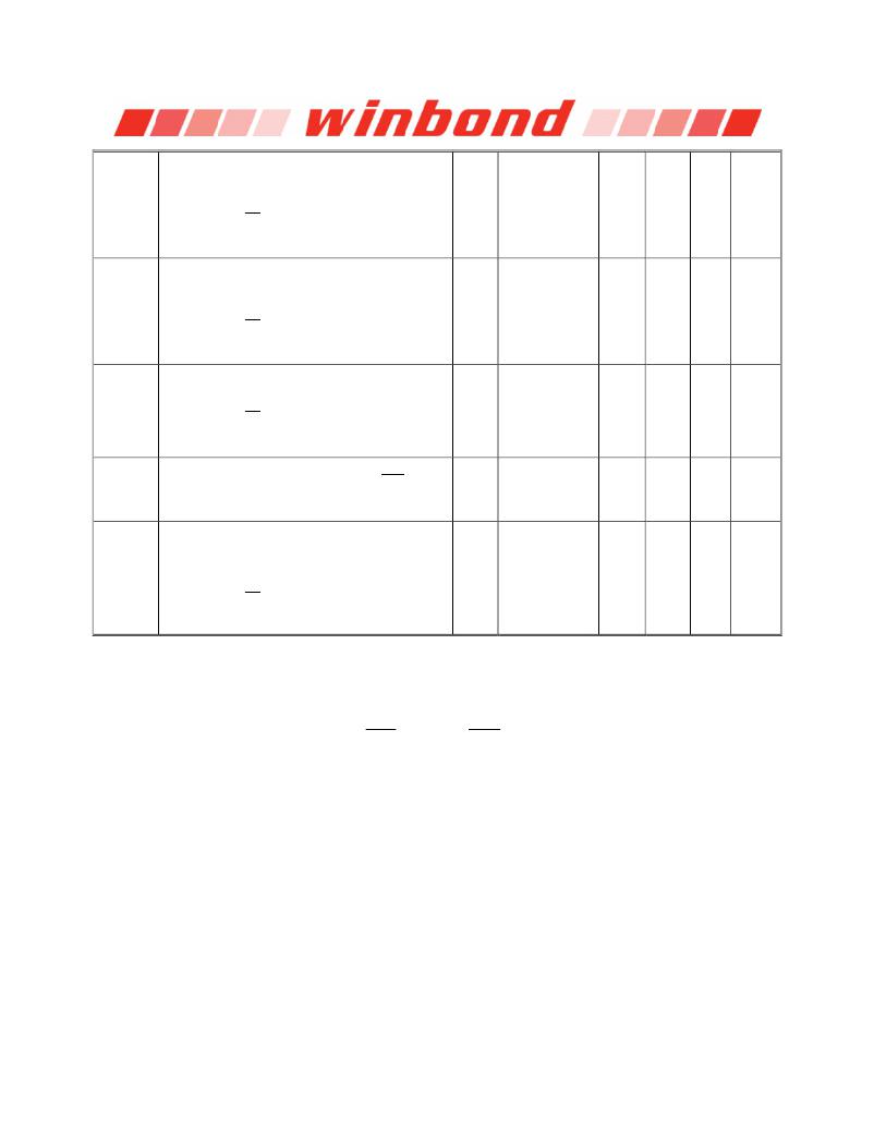
�Operating� Burst� Read� Current�
�All� banks� open,� Continuous� burst� reads,� I� OUT� =� 0� mA;�
�BL� =� 4,� CL� =� CL� (IDD),� AL� =� 0;�
�I� DD4R�
�t� CK� =� t� CK(IDD)� ;� t� RAS� =� t� RASmax(IDD)� ,� t� RP� =� t� RP(IDD)� ;�
�CKE� is� HIGH,� CS� is� HIGH� between� valid� commands;�
�155�
�130�
�130�
�120�
�mA�
�1,2,3,�
�4,5,6�
�Address� inputs� are� SWITCHING;�
�Data� Bus� inputs� are� SWITCHING.�
�Operating� Burst� Write� Current�
�All� banks� open,� Continuous� burst� writes;�
�BL� =� 4,� CL� =� CL� (IDD),� AL� =� 0;�
�I� DD4W�
�t� CK� =� t� CK(IDD)� ;� t� RAS� =� t� RASmax(IDD)� ,� t� RP� =� t� RP(IDD)� ;�
�CKE� is� HIGH,� CS� is� HIGH� between� valid� commands;�
�160�
�135�
�135�
�125�
�mA�
�1,2,3,�
�4,5,6�
�Address� inputs� are� SWITCHING;�
�Data� Bus� inputs� are� SWITCHING.�
�Burst� Refresh� Current�
�t� CK� =� t� CK(IDD)� ;�
�I� DD5B�
�Refresh� command� every� t� RFC(IDD)� interval;�
�CKE� is� HIGH,� CS� is� HIGH� between� valid� commands;�
�145�
�130�
�130�
�120�
�mA�
�1,2,3,�
�4,5,6�
�Other� control� and� address� inputs� are� SWITCHING;�
�Data� bus� inputs� are� SWITCHING.�
�Self� Refresh� Current�
�I� DD6�
�CKE� ?� ≤� 0.2� V,� external� clock� off,� CLK� and� CLK� at� 0� V;�
�Other� control� and� address� inputs� are� FLOATING;�
�Data� bus� inputs� are� FLOATING.� (T� CASE� ≤� 85°C)�
�10�
�10�
�4�
�10�
�mA�
�1,2,3,�
�4,5,6,�
�7�
�Operating� Bank� Interleave� Read� Current�
�All� bank� interleaving� reads,� I� OUT� =� 0mA;�
�BL� =� 4,� CL� =� CL� (IDD),� AL� =� t� RCD(IDD)� -� 1� x� t� CK(IDD)� ;�
�I� DD7�
�t� CK� =� t� CK(IDD)� ,� t� RC� =� t� RC(IDD)� ,� t� RRD� =� t� RRD(IDD)� ,� t� FAW�
�=� t� FAW(IDD)� ,� t� RCD� =� t� RCD(IDD)� ;�
�285�
�225�
�225�
�195�
�mA�
�1,2,3,�
�4,5,6�
�CKE� is� HIGH,� CS� is� HIGH� between� valid� commands;�
�Address� bus� inputs� are� STABLE� during� deselects;�
�Data� Bus� inputs� are� SWITCHING.�
�Notes:�
�1.�
�2.�
�3.�
�4.�
�V� DD� =� 1.8� V� ±� 0.1V;� V� DDQ� =� 1.8� V� ±� 0.1V.�
�I� DD� specifications� are� tested� after� the� device� is� properly� initialized.�
�Input� slew� rate� is� specified� by� AC� Parametric� Test� Condition.�
�I� DD� parameters� are� specified� with� ODT� disabled.�
�5.� Data� Bus� consists� of� DQ,� LDM,� UDM,� LDQS,� LDQS� ,� UDQS� and� UDQS� .�
�6.� Definitions� for� I� DD�
�LOW� =� V� in� ≤� V� IL� (ac)� (max)�
�HIGH� =� V� in� ≥� V� IH� (ac)� (min)�
�STABLE� =� inputs� stable� at� a� HIGH� or� LOW� level�
�FLOATING� =� inputs� at� V� REF� =� V� DDQ� /2�
�SWITCHING� =� inputs� changing� between� HIGH� and� LOW� every� other� clock� cycle� (once� per� two� clocks)� for� address� and�
�control� signals,� and� inputs� changing� between� HIGH� and� LOW� every� other� data� transfer� (once� per� clock)�
�for� DQ� signals� not� including� masks� or� strobes.�
�7.� The� following� I� DD� values� must� be� derated� (I� DD� limits� increase),� when� T� CASE� ≥� 85°C� I� DD2P� must� be� derated� by� 20%;�
�I� DD3P� (slow)� must� be� derated� by� 30%� and� I� DD6� must� be� derated� by� 80%.� (I� DD6� will� increase� by� this� amount� if� T� CASE� <� 85°C�
�and� the� 2X� refresh� option� is� still� enabled)�
�Publication� Release� Date:� Sep.� 24,� 2013�
�-� 41� -�
�Revision� A09�
�发布紧急采购,3分钟左右您将得到回复。
相关PDF资料
W971GG8JB-25
IC DDR2 SDRAM 1GBIT 60WBGA
W9725G6IB-25
IC DDR2-800 SDRAM 256MB 84-WBGA
W9725G6JB25I
IC DDR2 SDRAM 256MBIT 84WBGA
W9725G6KB-25I
IC DDR2 SDRAM 256MBIT 84WBGA
W972GG6JB-3I
IC DDR2 SDRAM 2GBITS 84WBGA
W9751G6IB-25
IC DDR2-800 SDRAM 512MB 84-WBGA
W9751G6KB-25
IC DDR2 SDRAM 512MBIT 84WBGA
W9812G6JH-6I
IC SDRAM 128MBIT 54TSOPII
相关代理商/技术参数
W971GG6JB-25I
制造商:Winbond Electronics 功能描述:-40~85 1GB DDR2 FOR INDUSTRY
W971GG6JB25ITR
制造商:Winbond Electronics Corp 功能描述:1G, DDR2-800, X16, IND TEMP
W971GG6JB25TR
制造商:Winbond Electronics Corp 功能描述:NR, DDR2-800, X16
W971GG6JB-3
制造商:Winbond Electronics Corp 功能描述:1GBIT DDRII
W971GG6KB-18
制造商:Winbond Electronics Corp 功能描述:1G, DDR2-1066, X16 制造商:Winbond Electronics Corp 功能描述:IC MEMORY
W971GG8JB
制造商:WINBOND 制造商全称:Winbond 功能描述:16M × 8 BANKS × 8 BIT DDR2 SDRAM
W971GG8JB-25
功能描述:IC DDR2 SDRAM 1GBIT 60WBGA RoHS:是 类别:集成电路 (IC) >> 存储器 系列:- 标准包装:72 系列:- 格式 - 存储器:RAM 存储器类型:SRAM - 同步 存储容量:4.5M(256K x 18) 速度:133MHz 接口:并联 电源电压:3.135 V ~ 3.465 V 工作温度:0°C ~ 70°C 封装/外壳:100-LQFP 供应商设备封装:100-TQFP(14x20) 包装:托盘
W9725G6IB-25
功能描述:IC DDR2-800 SDRAM 256MB 84-WBGA RoHS:是 类别:集成电路 (IC) >> 存储器 系列:- 标准包装:1,000 系列:- 格式 - 存储器:EEPROMs - 串行 存储器类型:EEPROM 存储容量:4K (512 x 8) 速度:400kHz 接口:I²C,2 线串口 电源电压:2.7 V ~ 5.5 V 工作温度:-40°C ~ 85°C 封装/外壳:8-SOIC(0.173",4.40mm 宽) 供应商设备封装:8-MFP 包装:带卷 (TR)